
Daisy’s
Theorem
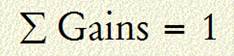
Daisy’s Theorem states that the sum of ALL
voltage gains must be equal to one. A linear circuit with voltage inputs is
assumed.
Daisy’s theorem applies to system gains. It is independent of circuit implementation. The theorem can reveal some circuit properties such as sensitivity to ground noise, the dependence between bandwidth and power supply noise rejection, etc. A less technical description is on the Daisy page.
Linear Circuit
A linear circuit can be represented by the equation:
V(out) = g1 V1 + g2 V2 + g3 V3 + … + gn Vn
Where:
V(out) is the output voltage,
Vi are the input voltages, and
Gi is the gain from the input to the output.
The circuit can be represented by the
schematic below:
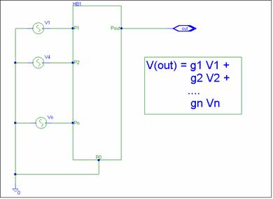
The circuit has voltage inputs, a
voltage output, and a ground reference. The ground reference is zero
volts and can not contribute to the output. Practical circuits have some
noise voltage on the ground node. We can represent this voltage by source
V0.
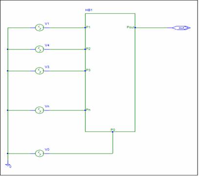
V(out) = g1 V1 + g2 V2 + g3 V3 + … + gn Vn + g0 V0
A better circuit
representation is shown below:
Below are some are
requirements for Daisy’s theorem.
HB1 can be any valid linear circuit. Not all schematics are valid circuits. Some circuits have undefined gains, some violate circuit rules. A circuit that shorts inputs or that has no connection from any input to the output, is not a valid circuit.
All inputs to HB1 must be shown. The schematic must be complete.
HB1 must have at least one input.
Ground and Supply voltages are inputs and must be shown as inputs to HB1.
All inputs must be ideal voltage inputs. All source impedances associated with the inputs are included in HB1. Current source inputs must be converted to voltage source inputs.
The circuit output is a node Pout. Pout can be any node in HB1. V(out) is the voltage at Pout. Any loading is included in HB1.
The gain, gi, is the voltage gain from voltage source input Vi to output V(out). G0 denotes the gain from the ground node, the Ground Gain. The gain sum includes all inputs gains. In addition to signal gains, the gain sum includes ground and power supply input gains.
Given the above constraints Daisy’s Theorem states that the sum of all gains is equal to one.
g1 + g2 + g3 + ... + gn + g0 = 1
Although the signal gains can have any value, including complex values, the sum of all the gains is equal to one. The sum of the gains is equal to one for all frequencies.
A gain of one denotes that the signal has not been changed. It has not been amplified nor attenuated. A gain of one is hence no gain. If you interpret the gain sum as the net gain, then circuits can not have net gain, or net loss. Active circuits have the same net gain as passive circuits, namely none.
Proof
A proof of Daisy’s Theorem is left as an exercise for the reader.[1] If a Spice simulator is available, you can test Daisy’s Theorem via an AC Simulation of your Circuit. Connect AC sources of magnitude 1 to all inputs, including ground and power supplies.
Have the simulator calculate the value of V(out).
V(out) = g1 V1 + g2 V2 + g3 V3 + … + gn Vn + g0 V0
With V1 = V2 = V3 = … Vn = V0 =1.
V(out) = g1 + g2 + g3 + … + gn + g0
The value that the simulator calculates for the output voltage is equal to the sum of the gains. The output should be equal to one for all frequencies. Make circuit changes and rerun the simulation.
If the output is not equal to one, check for
internal ground connections. Some op-amp models contain internal ground nodes.
Check the model. Also check that all input sources have their negative node
connected to ground.
Op-Amp Amplifier Power Supply Noise Rejection
Op-amp circuits have a finite bandwidth. The power supply noise rejection tends to become worse for frequencies above the bandwidth. Is there a correlation between circuit bandwidth and power supply noise rejection?
Answer: Yes. The decrease in circuit gain is compensated by an increase in the gain from the power supply leads.
Let’s test the answer via simulation. The
schematic of a Buffer amplifier is shown below:
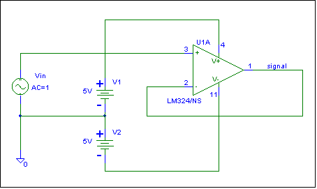
Be sure to use an op-amp model, such as the
National Semiconductor LM324/NS model, which does not use an internal
ground. The AC simulation output is shown below:
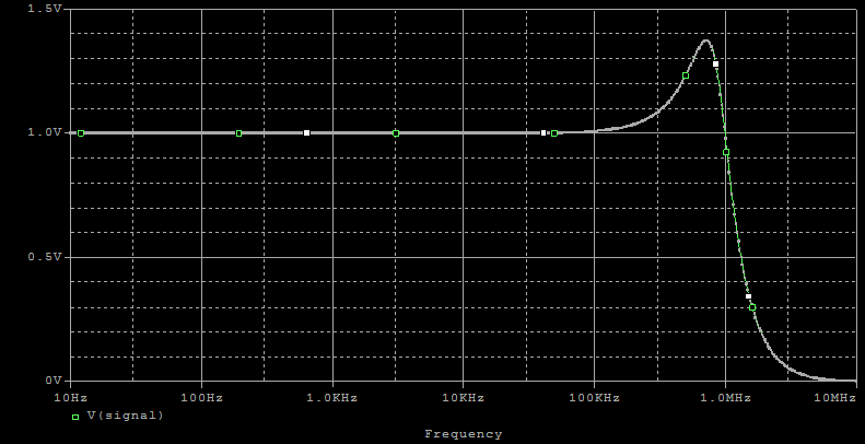
The AC response is the output for an input of magnitude 1. It is also the signal gain.
The circuit for measuring the Power Supply
Rejection is shown below:
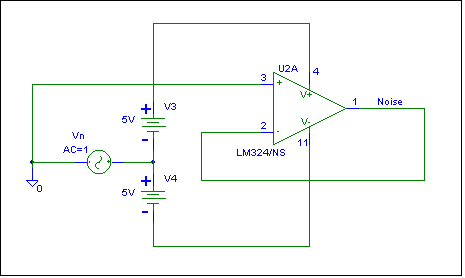
An AC source of magnitude 1 has
been connected between ground and the power supply common. The AC
simulation of the output is shown below:
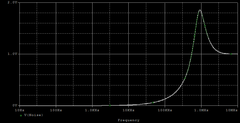
Since the input magnitude is one, the output is the gain. The plot tends to confirm Daisy’s theorem. For low frequencies the signal gain is equal to one and the noise gain is equal to zero. For high frequencies the signal gain is equal to zero and the noise gain is equal to one. In the transition area the sum does not appear equal to one. Let’s have the simulator calculate all.
The plot below shows the signal gain, the
noise gain, and the sum of the gains.
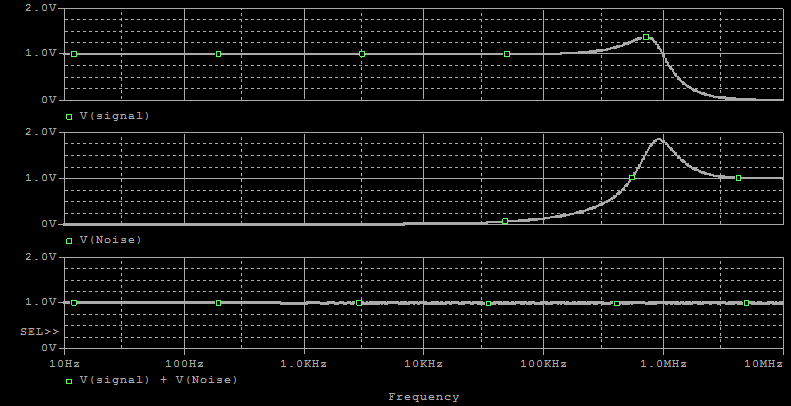
The sum is exactly equal to one. The plots show only the magnitude of the signals. When adding signals, the Simulator perform a vector sum of the signals.
Daisy’s theorem appears to be valid.
Summary and Conclusion
Daisy’s Theorem states that the sum of the circuit gains is equal to one. Daisy’s theorem allows the ground gain to be calculated from the signal gains. Knowledge of the circuit is not required.
Daisy is no longer with us. This theorem is dedicated to Daisy. To honor her, I ask that you keep the name.
There are many applications of Daisy’s Theorem. If you find a novel application or have questions, I can be reached at k9analysis@netzero.net.
[1] If the circuit is a passive circuit with a Thevenin Equivalent, then Daisy’s theorem is easy to prove via the conversion to a Norton Equivalent. I have been told that Daisy’s theorem is easy to prove for Op-amp circuits. I have never seen a proof for the general case. I have also never seen an exception.