Single
Op-amp Analysis Examples
On this page some single op-amp circuits are analyzed. The first step is to verify that the circuit is a subset of the General Summing Amplifier. The second step is to identify the Feedback Impedance, Zf. Determine the op-amp input node impedances, ZP+ and ZP-. Next identify the inputs and input Impedances. Apply Plato’s Gain formula for each input and sum the terms to get the output equation.
Ground is an input. Since the signal amplitude is equal to zero, it creates a zero term in the output equation. If you add the term, you can use Daisy’s Theorem to check your answer. If a single gain is difficult, you may to want to calculate the other gains and use Daisy’s Theorem for the difficult gain.
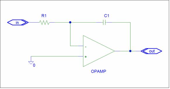
Buffer Amplifier
A buffer amplifier is the simplest single op-amp circuit. Does Plato’s Formula apply? Let’s investigate. The schematic for a buffer amplifier is shown below.
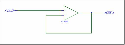
The circuit is a General Summing Amplifier with Zf and Zp equal to zero. A circuit impedance is never equal to zero. Even a short wire has some impedance. A better schematic is:
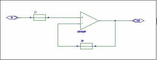
This is a General Summing Amplifier with
Zf= Zf ZP+ = Z1 ZP- = Zf
The circuit has one input with input impedance Z1 and gain Zf/Z1 * ZP+/ZP-.
Vout =
(Zf/Z1 * ZP+/ZP-) Vin
Vout =
(Zf/Z1 * Z1/Zf )Vin
Vout= Vin
Plato’s Gain
Formula works for a buffer amplifier.
Non-Inverting Amplifier
The application that
raises the most skepticism is the Non-Inverting Amplifier.
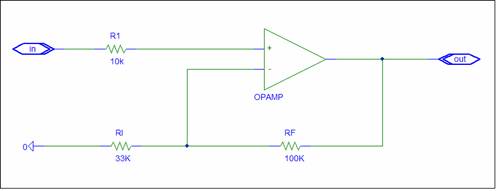
This circuit is a
General Summing Amplifier.
Zf = RF = 100K ZP+
= R1 = 10K ZP-
= R1 // RF = 25K p=
10k/25k = 0.4
This circuit has one
positive signal input, Vin with input impedance
R1.
The gain is RF/R1 * ZP+/ZP- = 100K/10K*0.4 = 4
Vout = (RF/R1 * ZP+/ZP- )*Vin
Rearranging and
expanding the ZP- term yields:
Vout/Vin
= RF/R1 * ZP+/ZP- = RF/R1 * R1/(RF//RI)
= RF / (RF*RI)/(RF+RI) = 1 +
RF/RI
= 1+100k/33K = 1+3 = 4
Note that since R1 =
ZP+; the R1 term and the ZP+ term cancel. The gain is not dependent on the R1
value.
Plato’s Gain
Formula only appears to be different.
In Plato’s gain formula, R1 is the positive input resistor. RI is a negative input resistor.
An alternate
approach is to use Daisy’s theorem. Daisy says the sum of the gains must
equal to +1. The circuit has a
negative ground gain and a positive signal gain. The negative ground gain is
–RF/RI = -3. The positive gain
needed to make the gain sum equal to one is 1+RF/RI = 4.
Plato’s Gain
Formula is a compact equation that applies to the General Summing Amplifier. It may not be the simplest form. In the case of the Non-Inverting
amplifier, R1=ZP+ and the equation reduces to the Legacy formula.
Plato intentionally
hides the 1+ RF/RI term. He wants
you think of gain as Rf/Ri times a fudge factor.
The 1+RF/RI formula suggests that the positive gain is greater than
one. This is true for the gain from
the (+) op-amp input, but not always true for the gain from a positive input.
Positive gains less than 1 pose no problem in K9.
The formula is for a
single positive input; R1=ZP+ is imbedded in the concept. Multiple positive inputs violate the
assumption and need special attention.
Legacy typically uses a two stage analysis, an input attenuator and the
1+RF/RI op-amp gain formula. The result is a complicated positive
gain equation.
Op-amp circuit
analysis can be Dog-Gone Simple if you use the 1+RF/RI formula
only for special case. Let’s
look at another example.
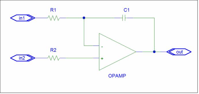
Differential Amplifier
A differential
amplifier is used to amplify the difference of two input signals. The circuit has a positive input and a
negative input with equal gain magnitude.
If the inputs have equal common mode components, then the output will
have no common mode component. The
Differential Amplifier is mainly used to cancel undesirable common mode
component in the inputs.
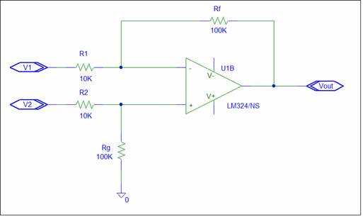
The circuit is a General Summing Amplifier.
Zf = Rf = 100K ZP+ = R2 // Rg = 9K ZP- = Rf // R1=
9K p=1
The circuit has two inputs;
V1 is a negative
input with Zni = R1 and gain = -Rf/R1 = -100k/10K =
-10
V2
is a positive input with Zpi = R2 and gain =
Rf/R2*ZP+/ZP- = 100K/10K = 10
Vout = – RF/R1*V1
+ Rf/R2 (ZP+/ZP-)*V2
The Differential
amplifier equation from Wikipedia is:
Vout = V2
( (Rf+R1) Rg / (Rg + R2) R1) – V1 Rf/R1
The equations are
the same. With
R1 = R2
and Rf = Rg
Vout =
Rf/R1 (V2 – V1) = 10 (V2 – V1)
Differential
amplifiers are used to amplify the difference of two inputs. To amplify only the difference you need
equal positive and negative gain magnitudes. You need R1 = R2 and Rf
= Rg.
A practical circuit
may need AC coupling for the inputs and high frequency noise attenuation.
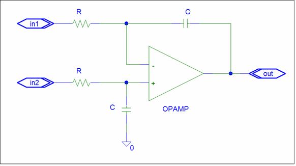
AC Differential Amplifier
Legacy texts always
use resistors. This is fine for
DC. What about AC. The schematic below is intended to be an
AC Differential Amplifier.
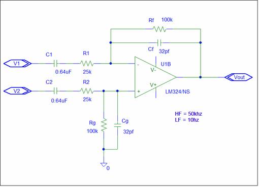
The first analysis
step is to identify the circuit Impedances.
The feedback
impedance, Zf, is the two terminal network
that connect the output to the (-) op-amp input.
Input impedances
connect from the input to an op-amp input.
Ground is an input.
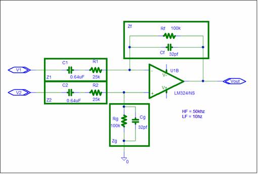
The circuit is a
General Summing Amplifier.
Zf = Rf//Cf ZP+
= Z2 // Zg ZP-
= Zf // Z1
The circuit has two
inputs.
The
negative input V1 has Zn1 = Z1 and gain = -Zf/Z1
The
positive input V2 has Zp1 = Z2 and gain = Zf/Z2 * ZP+/ ZP-
V1 is a negative
input; V2 is a positive input. The
output is;
Vout =
(-Zf/Z1)*V1+ (Zf/Z2* ZP+/ZP-)V2
ZP+ = Zf // Z1
ZP- = Z2 // Zg
In this schematic Z1
and Z2 are the same network. Zf and Zg are also the same network.
For Z1 = Z2 and Zf = Zg , ZP+ = ZP-
Vout = Zf/ Z1 (V2 – V1)
The Zf and Z1 impedances determine the frequency resonse. In the
mid-band, the gain is Rf/R1 = 4.
C1 and R1 form a
high pass filter; Cf and Rf form a low pass filter. The w= 1/RC formula from
K9 AC Analysis can be used for the breakpoints.
LF = 1 / ( 2*pi*25K*0.64uF)
= 10 hertz
HF = 1 / ( 2*pi*100K*32pF)
= 50Khz
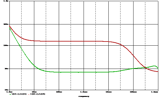
The simulation
schematic below contains two circuits to allow the positive and negative gain
to be displayed on the some output plot.
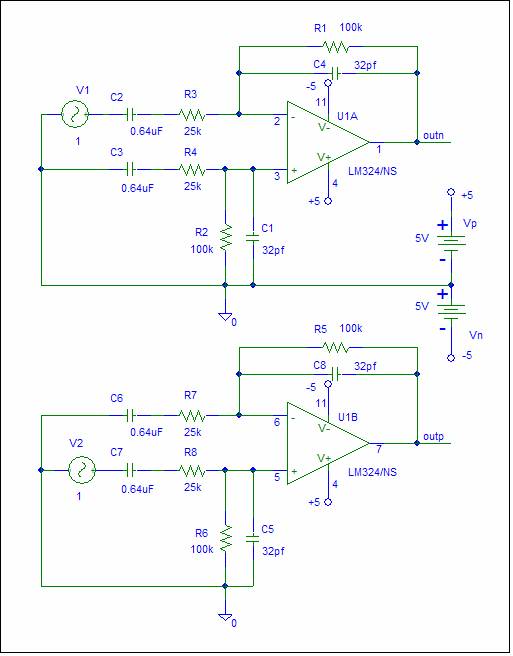
In the top circuit,
the input is applied to the negative input and the positive input is
grounded. In the bottom circuit, the
input is applied to the positive input and the negative input is grounded. The input magnitude is set to one to
make the output equal to the gain.
The simulation output is shown below:
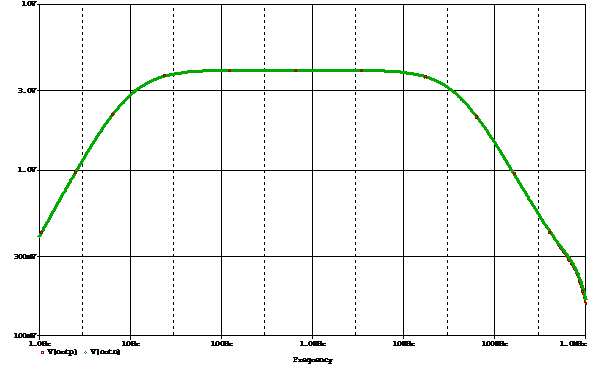
The gains are
equal. The mid-band gain = 4.
The slight difference
at 1Mhz is due to the op-amp gain. The assumption of large gain is no
longer valid.
This partially
validates Plato’s Gain Formula.
If the circuit is
designed with ZP+ = ZP-, the only difference between positive and negative gain
is the op-amp input terminal that the input is connected to.
Although the above
is true, there is a difference. The
input impedances are not equal. The
simulation calculation is shown below:
Telecommunication circuits
require that both the gain and input impedance be precisely equal to cancel
longitudinal (common mode) signals.
You will need a different circuit.
Modern interfaces also make the Impedances software selectable. For this you’ll need a DIGITAL signal
processor. We need to keep analog simple.
Integrator
Integrators are used in Analog Computers. A schematic is shown below.
This a General summing Circuit.
Zf = 1/sC1 ZP+ = 0 ZP- = R1 // Zf
The circuit has one negative input, Zn1 = R1. The gain is –Zf/Zi = -1/s R1 C1
Vout = 1/s (-1/R1*C1) Vin
This circuit has a problem. Zf becomes infinite at DC. You need to add a bleed-off resistor in parallel with C1 or provide some reset mechanism to create an initial output value.
This circuit has a negative gain. Is it possible to design a positive gain integrator? How about a differential input integrator? If you try to use 1+RF/RI, this will be very difficult. If you use Plato’s Gain formula, it’s easy. Here’s how:
Add a positive input.
Zf = 1/sC1 ZP+ = R2 ZP- = R1 // Zf
The circuit is not balanced. We need a capacitor connected to the (+) input and we need R1 = R2.
This is a General Summing amplifier.
Zf = 1/sC ZP+ = R // 1/sC ZP- = R // 1/sC p=1
The circuit has a negative input, in1, with gain = -ZF/Zi = -1/sRC
The circuit has a positive input, in2, with gain = pZf/Zi = 1/sRC
Vout = 1/sRC (V(in2) – V(in1))
Does this work? Let’s simulate the circuit.
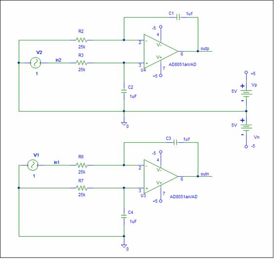
The schematic contains two copies of the circuit. In the top circuit the input is applied to in2 with in1 grounded. In the bottom circuit, the input is applied to in1 with in2 grounded. The simulator sets the initial capacitor voltages to zero, calculates a bias point, and performs an AC simulation.
The simulation output plotted on a log log scale is:

The gain shape is that of an integrator, gain decreases linearly with frequency.
The outputs overlap, except for high frequencies, where is op-amp gain becomes significant. The op-amp was changed from an LM324 to an AD8051 to improve circuit performance.
This partially
validates Plato’s Gain Formula.
If the circuit is
designed with ZP+ = ZP-, the only difference between positive and negative gain
is the op-amp input terminal that the input is connected to.
Single op-amp
circuit analysis can be Dog-Gone Simple if you use Plato’s Gain formula.