Stability
This page discusses stability in a K9 manner. No s-domain
analysis, but complex phase is used. Circuit simulation results are shown.
Apply the standard disclaimer to these results.
There are lots of misconceptions concerning stability. This page
attempts to clarify some concepts.
The remainder of the page looks at the stability of the General Summing Amplifier in complex
detail.
Trial Amplifier
On the Legacy page, the legacy analysis
procedure was applied to a new circuit. The Trial Amplifier was created by
reversing the op-amp connections in an inverting amplifier.

The Legacy analysis concluded that this circuit is not the
non-inverting amplifier desired but another inverting amplifier.

Let’s use the K9 VSA procedure to analyze the circuit. The SFG is
shown below:

A is the op-amp gain. The op-amp (-) input is ground and not shown
for simplicity.
ZP+ = RI // RF
The SFG has one loop with gain L.

The loop gain is positive and greater than one for A > 1 + RF/RI.

∆ is negative for values of A > 1 + RF/RI.
The SFG has one path from Vin to Vout.
The path touches the loop. No numerator correction is needed, just the ∆
denominator correction.

The analysis result is the same as the Legacy
analysis result. This appears to be an inverting amplifier. The signal flow
shows a single positive gain path from Vin to Vout.
How is negative gain possible?
The answer is that it is not possible. Note that the inversion is
created by the ∆ correction, not the amplifier.
What happened?
A circuit analysis procedure uses circuit laws to model the
circuit. The analysis method then tries to find a solution to the equations.
Both the Legacy and SFG analysis procedures found the same solution. If the
analysis is valid there should be one solution. There is no problem here. The
math found a solution that satisfies all requirements.
The Trial circuit does not work as an inverting amplifier. If you
build and test the circuit, you’ll find that the output is stuck at a supply
rail. If you force the circuit to a solution point, you will find that all the
voltages match the solution. The circuit just does not like to stay at the
solution point. PSpice could not simulate the circuit because of
convergence problems. This is an unstable circuit.
Is the Trial amplifier a bad circuit?
There are many bad circuits in text books and on Web pages. What’s
rare is to have an author declare his circuit to be bad. So, the Trial
amplifier is a great digital circuit. Most analog circuits do not create a
clear digital output. They operate in the voltage range between logical one and
logical zero and create definite maybe outputs. The Trial amplifier only has
two output states and avoids unknown states, truly a great digital circuit.
The Trial amplifier name suggests an amplifier. A better circuit
name is an analog flip-flop. The set input is a large positive voltage. The
reset input is a large negative input.
An analysis only finds a solution to a set of equations. A
solution only implies that if you force the circuit into a solution point, all
the measured voltages and currents match the solution. The Trial amplifier
solution meets this criterion.
Stability Criteria
A different question is “What does the circuit do when disturbed”?
A circuit may return to the solution point or diverge away from
the solution point. If it returns, the circuit is stable, if it diverges, it is unstable.
You can use the Nyquist stability criterion , the Lyapunov stability, or other methods to check the
circuit stability.
In K9,
A
circuit is stable if ∆ is greater than zero.
Simple enough?
The Trial amplifier has a negative ∆ value and is unstable.
Dictionary
stable
The Freedictionary defines stable as:
“Resistant to change of position or condition; not
easily moved or disturbed”
The Trail amplifier meets
this definition far better than most stable analog circuits. The Trial
amplifier does not respond to small changes in the input and is not easily
disturbed. The Trial circuit is stable by the dictionary definition, and
unstable by the K9 definition.
In Mathematics and
Electronics stable means converge. You need to remember that the Electronic
definition of stable maybe in conflict with the dictionary definition. In K9,
stable means converge to a solution point.
Linear Operation
K9 assumes Linear operation. What does
this mean?
It means that the circuit can be described by a set of Linear equations.
It also means that the variable values are not bounded. Real circuits
are bounded. In
many circuits, voltage values may not exceed the power supply values. Current
values are also bounded.
What happens when a circuit tries to go out of bounds?
The answer is not in the linear analysis. At the boundary a new
set of equations apply. Further analysis is needed.
Oscillation
Oscillation is often associated with circuit stability. When a
circuit is trying to reach a new operating point, it may oscillate around the new
operating point. If the oscillation amplitude decreases, the circuit is stable.
If the oscillation amplitude increases the circuit is unstable.
Real passive circuits are stable. If the circuit is highly tuned,
it may oscillate for a while before settling down. Note that unstable means
diverge. In a real passive circuit, the oscillation magnitude can not increase
for many reasons. Power is one.
Active circuits have boundaries. An unstable circuit will
encounter a boundary as the oscillation magnitude increases. At this point the
linear analysis is no longer valid.
If you observe oscillation in your circuit, the circuit is
probably stable. Unstable circuits, like the Trial amplifier have sufficient
positive feedback to avoid oscillation. Unstable digital circuits can
oscillate, but not in the ringing manner of a stable analog circuit. An example
is the Relaxation
oscillator circuit.
Most digital circuits are intentionally unstable. Digital circuits
should have a clear digital output. Most include sufficient positive feedback
to make ∆ negative.
∆ Term
The ∆ term determines stability.
In K9, the ∆ term is the global system path correction. A
large negative value is a clear sign that the circuit is unstable and that the
circuit equation is not a good description of circuit operation.
A small positive ∆ creates a large amplification of the
circuit path gain. A ∆ value of 0.01 will increase the path gain by
100. A small positive ∆ may be valid
for a tuned passive circuit, but may be sign that an active circuit will go out
of bounds.
Tools
Stability is difficult to analyze. For an accurate analysis, you
need to be aware of circuit assumptions and tool limitations. Every tool has
limitations. Unfortunately, limitations are rarely discussed.
Electronics often uses simple procedures for circuit analysis. The
Legacy page showed how the elegant op-amp analysis
procedure failed for the Trial amplifier. The Trial amplifier is not an
INVERTING amplifier. The K9 VSA analysis procedure concluded that the Trial
amplifier is an unstable INVERTING amplifier. Signal
Flow indicates a NON-Inverting amplifier. The circuit is actually a
Flip-Flop, not an amplifier.
Electronics includes many theories that look good, but don’t model
an actual circuit. The lumped model of a
transmission line has never matched a real telephone line for me. You need
to verify your results with real circuit measurements!
Electronics and K9 VSA is limited to linear circuits. The
procedure can not determine circuit operating bounds. VSA assumes that op-amps
outputs are ideal voltage sources. You may need a better model that includes
op-amp output impedance. VSA allows stray capacitance to be included in node
impedances. You need to remember to include these stray components that are not
shown on the schematic.
An analog circuit simulator such as PSpice
can be a valuable tool. The AC analysis tool assumes linear operation. A
Transient simulation can show circuit bounds and non-linear operation. The
simulator is limited by circuit models. With poor models it becomes a trash
compactor: garbage in garbage out.
This applies also to Digital Simulators. PSpice
is a good digital simulator, but fails the Digital Simulator
Test . The test circuit consists of five two input NAND gates. To be fair,
all digital simulators fail the test.
How does one find the tool capabilities and limitations?
Don’t look for limitations in the tool description. Marketing does
an excellent job of hiding limitations.
There
are Lies, Dam Lies, Statistics, and Marketing.
The only good way to evaluate a tool is to test a real circuit and
check the tool results against circuit measurements. If the test does not match
the analysis, you need to make changes until the results match.
Tools are great. Just remember that when a tool fails, it’s your
fault.
Confused?
Let’s make things a bit more complex by looking at the General Summing amplifier in detail.
General Summing Amplifier
For op-amps circuits the analysis is a bit more complex because
the loop gain sign can change with frequency. For the General Summing amplifier :
|
|
|


D = 1 – L1 = 1 + A * ZP-/Zf
The above equation suggests that ∆ is positive and the
circuit is stable. If the loop gain is negative, the circuit will be stable. To
be unstable, the loop gain must be positive AND greater than one. If we look at
the ∆ equation in the complex domain, both A and ZP-/Zf
have complex values. If the phase shift of A and ZP-/Rf exceeds 180 degrees, than the loop gain becomes
positive.
For a real op-amp circuit, the loop gain phase will exceed 180
degrees at high frequencies. You need to make sure that your circuit model
includes the stray components that create this phase shift. If your model shows
that the phase shift does not exceed -180°, you need a better model.
For the general summing amplifier, the stability question is not
whether the loop gain changes sign, but what the gain magnitude is when this
happens. If the loop gain magnitude is
less than one, the circuit is stable.
Let’s look at the individual loop terms.
Op-Amp Gain
The open loop gain, A can be obtained from a data sheet or a
circuit simulation. You can use the circuit below to find A.

RF and C allow the simulator to create bias for the (-) op-amp
input. The input is a 1 volt AC signal. The Vout output is thus the op-amp
gain. In an AC analysis, the simulator assumes linear operation. The output
signal is unbounded, only 100,000 volts at 1 hertz. The AC sweep from 1 hertz
to 10 megahertz is shown below:

The green plot is the magnitude of Vout. The red plot is the phase
of Vout. The data matches the LM324 data sheet.
The DC gain is 100,000 (100db). The gain decreases above 10 hertz and is less
than one at 1 megahertz.
For stability, the gain needs to be decreased before the phase
changes sign. Most op-amps have an internal circuit that decreases the gain to
one before 180° phase shift occurs. The op-amp gain roll-off is set at 6db per
octave. When you double the frequency the gain is halved.
The red curve shows the phase. At DC, the phase is close to zero
and starts to decrease. The -6db magnitude slope creates a 90° phase shift. At
high frequencies, undesired components decrease the phase and make the gain slope
more steep.
The gain and phase are related via a Bode plot. Each reactive
component can alter the phase by 90° and the gain slope by 6db. A pole
decreases the phase and gain slope. A zero does the opposite. In the above gain
plot, there is a pole at 10 hertz and 500K hertz. The pole frequency
corresponds to a 3db gain change or a 45° phase change. As you sweep the
frequency from low to high, note that the phase changes before the gain slope
changes.
If the gain is less than one for phase below -180°, the op-amp is
unity gain stable.
When the op-amp phase changes from positive to negative, the
magnitude needs to be less than one for stable unity gain operation. Some
op-amps are only stable for a minimum specified closed loop gain. In this case
the ZP-/Zf term must provide the additional loop gain
attenuation.
Amplifier
Let’s investigate the case where the circuit impedances are
resistors.
|
|
|


D = 1 – L1 = 1 + A * ZP-/Zf
The ZP-/Zf term is gain from Vout to V-.
For resistors the phase is 0°. The magnitude is the inverse of the sum of
positive amplifier gains. For an inverting amplifier with gain of -5, the
positive gain is 6 and the magnitude of ZP-/Zf is
1/6.
A resistive amplifier is stable if the op-amp gain A is stable.
The ZP-/Zf term adds no phase shift and may only add attenuation.
The attenuation will make the amplifier more stable. The worse case is an
amplifier gain of one.
|
Buffer Amplifier
Let’s investigate a buffer amplifier. For an accurate analysis you
need to include stray circuit components. These are not on the circuit stock
list, but can be relevant to circuit performance. Each circuit node has some
capacitance to ground. This capacitance is part of the node impedance.
For analysis, we want to look at the loop gain and the transient
response.
The schematic below adds the feedback resistor to the op-amp
circuit above.

C3 and C4 are stray capacitance at the op-amp output and the inv
input.
The op-amp loop is broken at the inv input. The circuit measures
the loop gain by applying a 1 volt AC input to the positive op-amp input. The
op-amp output is connected to the feedback resistor, Rf. The inv node is not
connected to the negative op-amp input. R and C allow the simulator to
calculate a bias point. The AC simulation output is shown below:

The red plot is the gain and the green is the phase. For stability
the gain should be less than one when the phase is less than 180°.
If you want to avoid the oscillation you need to have sufficient Phase margin.
The Phase margin is difference in degrees between 180° and the
phase when the loop gain is one.
If the gain plot shows a phase of -145° when the gain is unity,
then the phase margin is 35°.
PSpice calculated a phase margin of 1.04 °.
The schematic below includes the stray capacitance at the (-)
op-amp input and stray output capacitance. PSpice is
set for feedback resistor values of 10k, 100k, and 1meg.

The table below shows the loop gain magnitude and phase plus the
pulse response to a 1volt input.
The gain plot is expanded around the unity gain point. Unity gain
and 180° phase is in the middle.
|
RF = 10k |
RF = 100k |
RF = 1meg |
|
|
|
|
|
PM = 23° |
PM = 1.04° |
PM= - 0.4° |
|
|
|
|


For stability the green loop gain needs to be less than one before
the red phase plot crosses 180°. In the 10k plot the green magnitude plot crosses
unity before the red phase plot. The 100k plot shows that the gain just crosses
before the phase. In the 1meg plot the crossing is close.
The buffer circuit includes stray capacitance. The Phase Margin
(PM), is 23° for a 10k feedback resistor, 1.04° for a
100k, and -0.4° for 1meg. A negative PM value implies unstable.
The pulse response shows some ringing for the 100k and 1meg case.
Since the oscillation dies down the circuits are stable.
The stray capacitance creates an additional pole. The pole
frequency can be found via

![]()
Where C is the stray capacitance value and R is the equivalent
resistance that C sees looking into the circuit.
For the (-) op-amp input, in this case R = Rf. In general R = ZP-.
|
RF=10k |
RF=100k |
RF=1Meg |
|
F=1.6Meg |
F=160K |
F=16K |
The pole frequency, F, determines the capacitance effect on circuit
operation. The pole adds attenuation and phase shift to the loop. The problem
is that the phase shift starts at a lower frequency than the attenuation. At F,
the pole adds a -45°phase shift. If A > 1 at F, the additional phase shift
will make the circuit less stable. If A < 1 at F, the additional phase shift
may have no effect.
In this example, the GBW is 1 Megahertz. The 10K resistor has F
> GBW and little effect. For the 100K resistor, F < GBW and the added
phase shift creates ringing. For the 1 meg resistor, F
<< GBW and pronounced ringing occurred.
For the amplifier case, the stray capacitance sees ZP-. For gains
greater than one, ZP- is less than Rf.
This will improve stability. Calculating the stray pole frequency is
an easy check. The location of the pole frequency, F, is very important. You
want F >> GBW.
When you use a higher GBW op-amp, this becomes more difficult. You
may have to reduce the feedback resistor to a lower value. Use Emma’s rule to scale the resistor values.
You also need to check the pole created by a capacitive load on
the op-amp output. A real op-amp has some output impedance. A 10nF output load
and a 25 ohm output impedance will create a 637K pole
frequency.
The buffer amplifier is the worst case for an amplifier. If the loop gain is less than one, when the loop gain phase exceeds
-180°, than the circuit is stable. To accommodate stray capacitance the
op-amp needs to have adequate phase margin.
Time Domain
The ringing response can be explained in the time domain by the
loop delay. The feedback loop has delay thru the op-amp and the feedback
network.
The op-amp forms the output from the differential input. Since the
loop creates a delay, the differential input will not immediately go to zero,
when the op-amp reaches the new operating point. When the feedback arrives at
the input, the output has overshot the desired output and needs to reverse to
attempt to converge to the final stable operating point.
If the loop delay is less then the signal rise time, the circuit
will have minimal overshoot.
You can quantize this behavior via an s-domain analysis.
In audio articles, negative feedback is often blamed for amplifier
distortion. This is false. Negative feedback is good. The problem is that the
feedback did not occur in real time. For minimum distortion the loop delay
should be less than the input rise time. This allows the feedback to control
the output. Another problem is that an audio circuit often has inadequate
signal range and goes out of bounds. When a circuit encounters a boundary, the
feedback looses control.
Let’s look at some reactive General summing amplifier circuits.
Differentiator
The intent of a differentiator circuit is to form an output which
is the derivative of the input. The schematic is shown below:

The circuit gain can be found from Plato’s
Gain Formula.

The s term denotes differentiation. In the frequency domain, the gain
increases with frequency and the phase is -90°. In the time domain, the output
is proportional to the input slope. Note the input inversion. A simulation
schematic is shown below.

The AC simulation output is shown below:

The green curve is the magnitude of Vout and the red curve is the
phase of Vout. The circuit has the desired increasing slope and -90° phase for
low frequencies. At 10k hertz, the gain peaks and the phase shifts to -270°. The
rapid change is warning that something occurred. This is almost always a bad
sign.
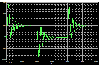
Let’s look at the transient response.

The green curve is the output and the red curve is the input. The
input initially rises. This should create a constant negative output. When the
input is constant, the output should be zero. The simulated output has some
resemblance to the desired output, but is not likely what you want.
To see the cause we need to look at ∆ and the loop gain.
D = 1 – L1 = 1 + A * ZP-/Zf

The 1/s term adds -90° to the loop phase. At low frequencies, the
A phase is -90°. This brings the circuit close to unstable. At high
frequencies, the loop phase will exceed -180°. We need a better circuit.
To create a stable circuit, we need to stop the differentiator
response at high frequencies. One way is to switch the circuit to an amplifier.
In the circuit below R1 is added.

For low frequencies, the Z(C) is greater than R1, and the circuit
is a differentiator. For high frequencies R1 is greater than Z(C), and the
circuit acts an amplifier with a gain of Rf/R1 = -10.
The AC simulation output is shown below:

The circuit retains the differentiator response for low
frequencies. The gain peak and phase jump at 10k hertz are gone.
Let’s look at the transient response.

Better, but not the desired response. We could try a slower input
or other circuit modifications.
Anybody that has built an Analog
Computer, will tell you to avoid differentiators.
An op-amp differentiator is a bad circuit.

The differentiator circuit is similar to an amplifier with a large
capacitance connected to the (-) op-amp input. The capacitor creates a low pole
frequency and circuit instability.
If your text book suggests that an op-amp differentiator is a
practical circuit, ask for a refund.
Let’s look at an integrator.
Integrator
The intent of an integrator circuit is to form an output which is
the integral of the input. The schematic is shown below:

The circuit gain can be found from Plato’s
Gain Formula.

The 1/s term denotes integration. In the frequency domain, the
gain decreases with frequency and the phase is +90°. In the time domain, the
output is proportional to the input slope. Note the input inversion. A
simulation schematic is shown below.

The AC simulation output is shown below:

The green Vout plot shows the desired decreasing slope and the red
curve shows the 90° phase shift. The Vout plot shows desired circuit operation
to 1mega hertz. The phase response is only the desired response to 10k hertz.
This is typical.
The Transient simulation response is shown below:

The circuit operates as desired, but has a DC output error. The
integrator needs some extra circuitry to create an initial value.
Integrators are very stable circuits. They are used in filter
circuits such as the State Variable Filter.
Summary
In Electronics, Stable means converge to a solution point.
Unstable circuits never reach the solution point and will encounter a circuit
boundary.
Circuit stability is determined by the value of ∆. ∆
is greater than zero for stable circuits. A low ∆ value creates a large
global correction term. This can cause a circuit to go out of bounds or create
ringing.
The General Summing Amplifier is stable for resistive circuits if
the op-amp is unity gain stable and the poles created by capacitance at the (-)
input and output are greater than the op-amp unity gain frequency. Capacitance
to ground at the (-) input can create instability.
Avoid differentiator circuits. Use integrators.
Check your analysis. Tools have limitations. Test your circuit!