General Summing
Amplifier
The General
Summing Amplifier is intended to be a generic single op-amp circuit. Many
op-amp circuits are a subset of the General Summing Amplifier. The circuit has
multiple inputs which are summed to create the output.
V(out) = Gp1*Vp1 + … + Gpn*Vpn – Gn1*Vn1 - … - Gnm*Vnm
Gpi is the gain from positive input i to V(out), and Gnj is the gain from negative input j to V(out). Each input
is an ideal voltage source. Non-ideal sources can be accommodated by including
the source impedance in the input impedance. The gain is the gain from the
ideal source impedance.
This circuit
forms an output which is the sum of gains times input voltages. It can
implement any linear circuit.
On this page the
circuit is analyzed for input to output gains.
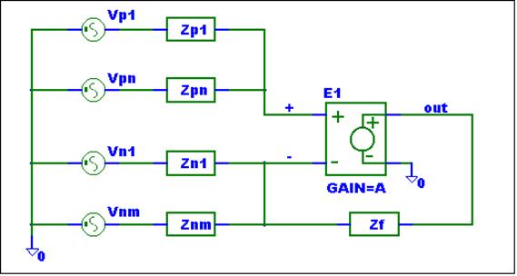
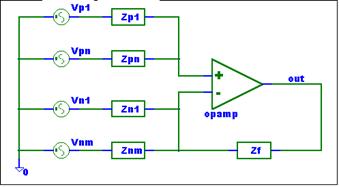
The General Summing Amplifier schematic is shown below:

The circuit can have multiple inputs. The positive inputs, Vpx, connect via positive input impedances, Zpx, to the "+" op-amp input. The negative inputs, Vny, connect via negative input impedances, Zny, to the "-" op-amp input. The circuit needs at least one positive input. Any input may be ground. Zni may not be equal to zero. Zpi or Zf may be equal to zero.
Even with the above
constraints, many op-amp circuits are a subset of the general summing
amplifier.
|
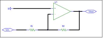
Inverting amplifier |
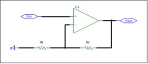
Non-Inverting Amplifier |
|
|
|
|
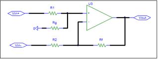
Differential Amplifier |
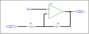
Integrator |
|
|
|
For example, an inverting
amplifier would have a single positive input that is ground and a single
negative input. A non-inverting
amplifier has a single positive input and a single negative input that is
connected to ground. A differential
amplifier has a positive and a negative input. Summing
circuits have multiple inputs. Since the feedback and input elements are
impedances, integrators
and differentiators
are also subsets of the General Summing Circuit.
Legacy Analysis
treats the subsets as separate circuits. In K9 Analysis, all of these circuits
are a type of General Summing Amplifier.
On this page, we will use the K9 VSA procedure to get the gain from the inputs to the op-amp
output.
Construct
Simulation Schematic
The first step in
the VSA procedure is to construct a Simulation Schematic. We need inputs to
stimulate the circuit, and a complete description. The above schematic complies
with the Schematic rules for layout, but needs an
op-amp model and node labels for the op-amp inputs.
The op-amp is
modeled as a voltage controlled voltage source with gain equal to A. Except for
gain, the op-amp is assumed to be ideal. The op-amp inputs need labels. The
non-inverting op-amp input is labeled "+". The inverting op-amp input
is labeled "-".
The simulation
schematic is shown below:
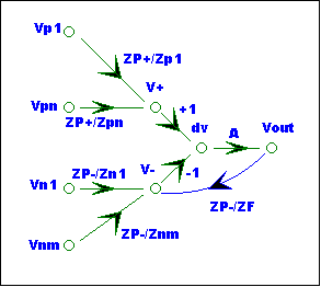
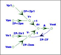
SFG
Construction
The next step is
to create a SFG. The VSA procedure uses the voltage at circuit nodes for SFG
variables. We want the SFG layout to match the schematic layout to retain the
signal flow. The SFG nodes are shown below.
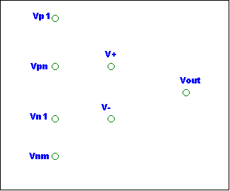
The nodes are
arranged to match the schematic.
The next step is
to add the controlled source to the SFG. The E source forms the difference of
the input voltages and amplifies the difference with gain A. In the SFG , dv is the difference
voltage.
dv = (V+) – (V-)
The op-amp
amplifies only the difference of the input voltages at the V+ and V- nodes. Any
common mode
component is rejected in this model. The differential input voltage is
amplified to create Vout. The amplifier gain A can be any value.
Vout = A * dv
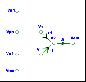
The dV node was added to implement the dv
equation. Both dv and Vout are voltage controlled
nodes. We simply added the defining equations to the SFG.
Vp1 to Vpn and Vn1 to Vnm are inputs.
These are known values and no defining equations are needed.
V+ and V- need to
be defined. Both are passive summing nodes. The node impedance and incoming
signals are needed.
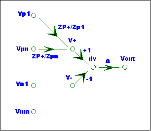
For V+, the
parallel impedance is:
ZP+ = ZP1 // … // ZPn
V+ receives
signals from the positive inputs. Brandy supplies the
branch gains. Each branch gain is equal to ZP+ divided by the connecting
impedance. The SFG with the V+ incoming branches is shown below:
The V- node is
also a summing node. The negative inputs and the op-amp output connect to V-.
The parallel impedance is:
ZP- = Zn1 // … // Znm
// Zf
V- receives signals from the negative inputs, Vnm, and the output, Vout. The SFG contains an incoming
branch for each input. Brandy
supplies the branch gains. The complete
SFG is shown below:
SFG Check
The input nodes
should not have incoming branches.
The summing
nodes, V+ and V-, should have incoming branches with branch gains equal to the
parallel impedance of the destination node divided by the branch impedance.
Vout is a
voltage-controlled node.
The signal flow
in the SFG matches the circuit schematic signal flow. There is a path from each
input to the op-amp output. Positive inputs have a positive path gain, while negative
inputs have a negative path gain. The SFG has a loop implying that path gains
need a correction.
Analyze SFG
The SFG has a
single loop. The loop contains the branches from V- to dv
to Vout to V-.
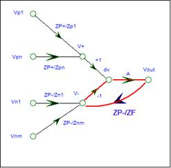
The loop gain is:
L1 = - A * ZP-/Zf
The determinant D is:
D = 1 – L1 = 1 + A * ZP-/Zf
The D term is the denominator correction factor
for path gains. As long as D is
positive and does not become zero, the circuit is stable. The above D term contains only positive values. This is
good. There is a catch. For many op-amps, the gain A has a 90° phase shift. If
the ZP-/Zf term has another 90° phase shift, problems
can arise. Look at the Stability page.
The SFG contains
multiple inputs. Superposition
is used to find the gain from a single input with the other inputs equal to
zero. In Electronics you need to ground the un-used voltage inputs. K9 does
this for you automatically. There is no need for another circuit. Mason’s Gain Formula
assumes that you are using Superposition.
The gain formula applies for the gain from a single input to an output with all
other inputs equal to zero.
Positive Input
Let’s find the
gain from positive input Vp1 to the output. The SFG has a single path from Vp1
to Vout.
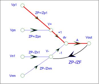
The path is from
Vp1 to V+, to dv, to Vout. The path gain is the
product of the branch gains:
P(Vp1 -> Vout) = ZP+/Zp1 * 1 *A
The SFG contains
a loop. The ∆ correction is needed. When we remove the path from the SFG,
the resulting SFG has no loops. The numerator correction is hence equal to one.
The gain from Vp1 to Vout is:
Gp1 = Vout/Vp1 = (A * ZP+/Zp1) / (1 + A *
ZP-/Zf)
The above formula
is the gain from Vp1 to Vout with all other inputs equal to zero. Superposition is
implied in Mason’s Gain
Formula . The K9 procedure does this automatically. The formula assumes
that you have replaced all other voltage inputs with ground. You need to
remember to do this when testing a real circuit.
In a similar manner, the gain from Vpn
to Vout is:
Gpn = Vout/Vpn = (A
* ZP+/Zpn) / (1 + A * ZP-/Zf)
Whenever you see
a Vout/Vpn term, reads this as the contribution to
Vout from Vpn. The circuit can have additional inputs
that contribute to the Vout value. K9 finds these one input at a time.
Negative Input
The gain for a
negative input to the output can be obtained from the SFG in a similar manner.
In this case the path goes thru V- rather than V+.
Input Vn1 has a
single path from Vn1 to Vout.
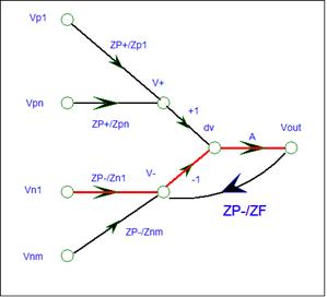
The path gain is:
P(Vn1 -> Vout) = ZP-/Zn1 * -1 *A
The SFG contains
a loop. The ∆ correction is needed. The path touches the loop, implying
that a numerator correction is not needed. The gain from Vn1 to Vout is:
Gn1 = Vout/Vn1 = (-A * ZP-/Zn1) / (1 + A *
ZP-/Zf)
In a similar manner,
the gain from Vnm to Vout is:
Gnm = Vout/Vnm =
(-A * ZP-/Znm) / (1 + A * ZP-/Zf)
The Vout value
can be found by adding all the input contributions.
V(out)
= Gp1*Vp1 + … + Gpn*Vpn –
Gn1*Vn1 - … - Gnm*Vnm
Check the
Answer
The above
equation include the op-amp gain, A. The ideal equations assume that the op-amp
gain is infinite. The ideal positive gain is:
Gpn = Vout/Vpn = ( ZP+/Zpn) / ( ZP-/Zf)
Rearranging the
term yields:
Gpn =Vout/Vpn = ( ZP+/ZP-) / ( Zf/Zpn)
The ideal positive
gain is ZP+/ZP- times the Feedback Impedance, Zf,
divided by the input impedance, Zpn.
The ideal
negative gain is:
Gnm = Vout/Vnm = (-
ZP-/Znm) / ( ZP-/Zf) = - Zf/Znm
The ideal
negative gain is the Feedback impedance divided by the input impedance.
The ideal
negative gain formula is the same as the Legacy negative gain formula. The
positive gain formula appears to differ from the 1 + Rf/RI
Legacy formula. With a single positive input, ZP+ is equal to Zpn. In the Legacy formula RI is a negative input resistor
connected to ground.
ZP- = Rf // RI = Rf * RI / (Rf + RI)
The ZP- term can
be expanded, as shown above, and substituted into the positive gain formula.
Gpn
= Vout/Vpn = ( ZP+/Zpn) / ( ZP-/Zf) = 1 / (Rf * RI / (Rf + RI)) / RF
With a little
algebra, the equation can be reduced.
Gpn
= Vout/Vpn =
1 / (RI / (Rf + RI)) = (Rf + RI) / RI = 1 + Rf / RI
The positive gain
formulas are the same. Note the difference in terminology. RI is actually a
negative input resistor.
Summary
The gain formulas
for the General Summing Amplifier were derived. The formulas contain a common Zf/Zi term and a fudge factor, p, that is
equal to ZP+/ZP- for positive inputs and –1 for negative inputs.
|
Circuit |
Signal Flow Graph |
|
|
|
The analysis used
Brandy’s Gain Formula to construct the SFG. This resulted in a combined gain formula
that is Plato’s Gain Formula.
Conclusion
K9 analysis
provides an easy way to analyze op-amp circuits. Instead of analyzing a
specific circuit, we chose a circuit that can represent many single op-amp
circuits.
The General
Summing Amplifier can be used to implement any Linear
circuit using only a Single op-amp. The two op-amp solution used in Electronics
is compared with this circuit on the Two Op-amp Circuit
page.
The Legacy approach assumes that dv
is equal to zero to simplify analysis. This creates separate formulas for
inverting and non-inverting circuits. Other single op-amp circuits also have
unique gain formulas. Leading to the conclusion that op-amp circuits are
difficult. K9 attempts to dispute the conclusion.
In the analysis,
ZP+ and ZP- are the node impedances at the op-amp inputs. K9 node impedances
assume that there is no circuit interaction (loops) .
The real circuit impedance is derived on the Op-amp
input page.
In a future page,
equations for the non-ideal op-amp parameter such as bias current, input offset
voltage, and output impedance may be derived. Look for The Ultimate Op-amp
Gain Formula.