Schematics
The intent of K9 Analysis is to make Analogue Circuit Analysis Dog-Gone-Simple. In K9, a circuit is a set of electronic components that has at least one input and at least one output. The circuit operation is described by signal flow from the input to the output. The most important element is a clear schematic.
There are many ways to describe a circuit. You can use a Schematic diagram , a Netlist, Circuit equations, or a Text Description. K9 describes circuit operation via signal flow. Inputs create stimuli which propagate thru the circuit and create an output. The schematic needs to show the signal flow to allow it to act as a circuit description. You really don’t want to write a long dissertation; do you?
A schematic can contain lots of information that is not relevant to the Analysis problem. A Circuit Diagram shows the components and interconnections of a circuit. This can be a schematic or a Netlist. A schematic is a graphical description of a netlist. Most engineers prefer schematics over netlists. Schematic capture tools create the netlist from the schematic.
The Schematic diagram layout is very important. You want to clearly illustrate the important information. You want to minimize wire crosses and create a pretty picture. A schematic should be a picture suitable for framing and provide an intuitive circuit description.
Schematic capture tools allow you to choose the information displayed. If the schematic is created for a Printed Circuit Board (PCB) you may want the component footprint displayed. The electronic component value is not relevant and may not be shown. In this case, the schematic layout should match the PCB layout. A PCB schematic is shown below.
|
Schematic |
Simulation Netlist |
|
|
.EXTERNAL INPUT Vin .EXTERNAL OUTPUT Vout R_R5 3 1 1k R_R4 Vout 3 1k C_C1 2 0 1n R_R3 Vin 1 1k R_R1 1 2 1k R_R2 3 2 1k |
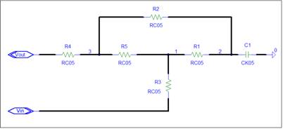
The schematic shows the board layout. The PCB inputs are on the left side of the PCB. The component placement matches the PCB placement. The components are labeled with their board footprint. The component values are hidden. The Simulation Netlist shows the component values, but not the package outline.
For Circuit Analysis, we want to show the information needed for analysis. This includes the component type and electrical value. Other data can be hidden. A simulation schematic contains the information needed to perform a circuit simulation. The PCB schematic lacks some information needed for simulation. The input signal is not defined, nor is the output load defined.
Simulation Schematic
For circuit analysis, additional elements are required. You need to show input sources and output loads on the schematic. Circuit operation depends on source impedance and load impedance. Without a clear definition, analysis is not possible. A good test is to submit the schematic to a Simulator program. The program will identify any errors and refuse to simulate a bad circuit.
A simulation schematic for the above circuit is shown below.
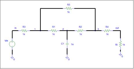
The schematic layout shows the Signal Flow in the circuit. Inputs are on the left and outputs are on the right. The circuit input signal travels from left to right across the schematic. This is what circuit do. They take input stimuli and propagate the input signals to the output. In a good schematic, the input to output signals propagate from left to right across the schematic.
In this case there are two direct signal paths from the input to the output. The input signal goes thru R3 to node 1, and thru R1, R2, and R4 to the output. The other path is thru R3, R5, and R4 to the output. Paths which go thru a node more than once don’t count. Signal flow is discussed in more detail on the signal flow page.
Discrete circuit schematic
K9 assumes linear circuit
operation. The voltage range is assumed to be large. Practical circuits are
limited by the power supply voltages. A schematic can display the voltage range
via the vertical placement of components.
The positive supply is at the top of the schematic and the negative supply is at the bottom of the schematic. The vertical component placement shows the component voltage. This is illustrated by the LM324 op-amp schematic shown below:
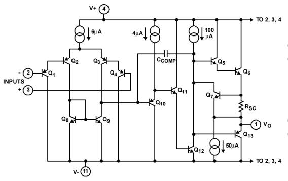
Components,
that connect to the positive supply,
are placed at the top in the schematic. Components that connect to the negative
supply are at the bottom. Note the transistor placement. PNP transistors have
the emitter on top, while NPN transistors have the emitter on the bottom.
The inputs and output are at
a potential between the supply voltages and shown in the middle. Voltage swings
are limited by the page boundary.
With proper placement,
current flows from the top of the schematic to the bottom. There should be no
exceptions.
The horizontal placement
shows the signal flow from input to output.
This is a good simplified
schematic. It clearly shows the basic circuit operation. Many details are not shown
for clarity. For this schematic, a detailed text description is not needed.
Additional information can be
shown on the schematic. The above circuit highlights compensation and current
limiting.
The current magnitude can be
shown via the line width. You can show large current paths via wide lines in
the schematic.
A schematic should be more
than a netlist. It can show many subtle circuit features. The rules are:
Signals flow from left to right.
Current flows from top to bottom.
You have a choice. Write a
text circuit description or let the schematic provide a clear circuit
description.
Signal Flow is discussed on
the Signal Flow page.
The SFG is discussed on the SFG page.