Ladder
Network Analysis
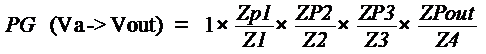
The schematic for a ladder network is shown
below. We want an equation for the input to output transfer function. The
equation should contain the component names to allow the component sensitivity
to be determined.
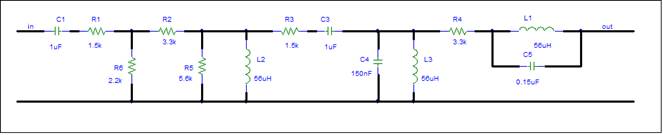
This circuit appears difficult because of the
large number of reactive components. When you look at the schematic, you can
see resonant circuits plus other potential difficulties. Am I going to need
calculus or complex variables? The answer is only if you want them. Electronics
can make circuits appear difficult. This is just an illusion. Don’t let the
schematic scare you.
The transfer function for the given set of
component values can be found via a breadboard test or a Simulation. You can
use Electronics circuit reduction with component values to get a simpler
circuit. Getting an equation for the transfer function is a bit more difficult.
Most sane engineers would not attempt to analyze this circuit via equations.
But since an equation is desired, let’s look at alternative procedures.
Various formal procedures are available, Nodal analysis, Mesh analysis, and State variable analysis.
The formal procedure provides a good opportunity to practice your algebra and
calculus.
The Electronics analysis procedure is to
reduce the circuit to simpler forms using series
parallel combinations. No calculus, but lots of complex algebra. The need
to keep the components as variables will make the equations large.
The K9 VSA procedure claims to make equation
derivation Dog-Gone-Simple. Let’s give it a try.
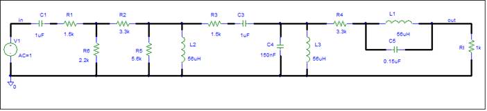
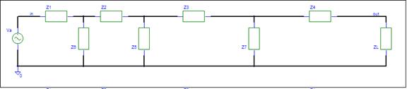
Construct the Simulation Schematic
The
schematic has no input and no output load.
An ideal voltage input is assumed. The output load is a 1K ohm resistor.
We can change this later to any two terminal impedance.
The simulator requires values for all components. It also needs a ground node.
The simulation schematic is shown below.
We
can check the schematic by running an AC Simulation. The output is shown below.
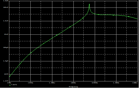
The
output is not important. Since the simulation ran, we can assume that the
schematic is valid.
Before starting the analysis, let’s look at
the circuit schematic more closely. The schematic shows lots of components
including several resonant sub-circuits (L3 C4 and L1 C5).
What about signal flow? The schematic
shows a single signal flow path. The vertical components only create
interaction. The horizontal components form a single signal path from the input
to the output. This is a good schematic for a simple circuit.
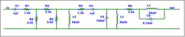
Construct the General Schematic
The next step is to reduce the schematic to a
general form.
This schematic
contains too much detail. Component values are not needed at the beginning. You
may want to note the component values. The values will be needed when the
equations are evaluated.
Some of the components can be lumped into 2
terminal Impedances. Lumping will reduce the number of components and usually
reduce the complexity of the answer.
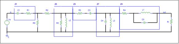
An Impedance can include one or more components. The lumped
components must form a two terminal network. R1 and C1 can be lumped into Z1.
R5 and L2 can be lumped into Z5, etc.
For each impedance record the passive network
that makes up the impedance. I like to make the impedance label the same as an included
resistor label if possible.
The input and output nodes are labeled. The
internal nodes need labels. The simulator automatically
assign hidden node names. We want a simple node assignment. The
schematic below has the internal nodes labeled 1, 2, and 3.
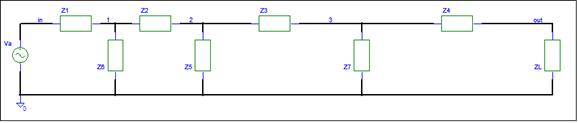
Note that the above circuit can represent
many ladder circuits. Any circuit, that has the above topology, 4 or less
series elements and 3 or less shunt elements, qualifies. The elements can be
any two terminal combination of components. You can remove
a series impedance by setting its value equal to zero.
You can remove shunt impedances by setting their value equal to infinity. We
are actually deriving the equation for a class of ladder networks.
The impedance schematic hides the reactive components.
You may think of an impedance as just a resistor. Just
remember to use the impedance value when evaluating any equation. The Signal Flow page shows that only horizontal
components matter in a VSA analysis. We now need to consider only Z1, Z2, Z3,
and Z4. There is a single path from the input to output. How difficult is the
Ladder circuit now?
The schematic is now acceptable for VSA
Analysis. Let’s get the gain equation.
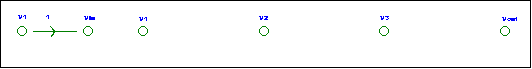
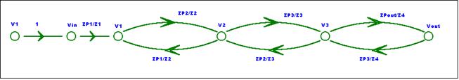
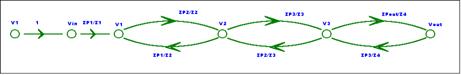
SFG Construction
The first step of SFG creation is to add SFG
nodes for the circuit nodes.
The nodes are arranged in the same pattern as
the schematic.
The ground node is not included, since the
ground voltage is equal to zero, it does not contribute to node voltage values.
Adding a ground node clutters the SFG.
The next step is to classify the circuit
nodes. In VSA there are two types of nodes: Voltage controlled nodes and
Passive summing nodes. Vin is a voltage-controlled
node. The Vin voltage is determined by the value of
the Va source, i.e.
Vin = Va
Or in SFG form
Vin = 1 *
Va
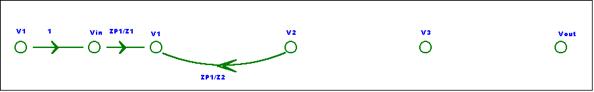
Add a branch from V1 to Vin.
Label the branch with the gain.
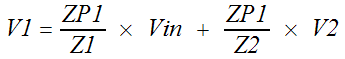
Node V1 is a summing node since no voltage
sources are connected to the node. Use Brandy’s Gain Formula to define the node voltage. First define the node
impedance, ZP1, at node 1. Impedances Z1, Z6 and Z2 connect to node 1.
ZP1 =
Z1 // Z6 // Z2
Next define the node voltage, V1.
You don’t have to write the equation for each
note. Just enter the terms into the SFG. The equation can be retrieved from the
SFG by adding the incoming branches. The equations are shown here for clarity
only.
Add two branches to the SFG, one from Vin to V1 with gain ZP1/Z1, the other from V2 to V1 with
gain ZP1/Z2. The branches are created by the circuit components. Z1 creates the
branch from Vin to V1. Z2 creates a branch from V2 to
V1. In each case the branch gain is the destination impedance, ZP1, divided by
the connecting impedance.
Z6 is a vertical
impedance. It connects from the node to ground. Since there is no ground node,
we do not have a SFG branch for Z6. You just need to include ground impedances
in the node impedance.
Repeat the above for node V2.
ZP2 =
Z2 // Z5 // Z3
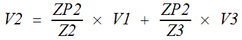
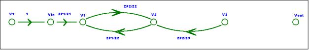
In the schematic V2 is connected to V1 and V3
via impedances Z2 and Z3. The SFG will
have incoming branches from V1 and V3. Brandy says
the branch gain is the destination impedance, ZP2 divided by the connecting
impedance. Z5 connects to ground. It is part of ZP2 but does not create a SFG branch.
V3 is also a summing node.
ZP3 =
Z3 // ZNC5 // Z4
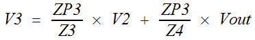
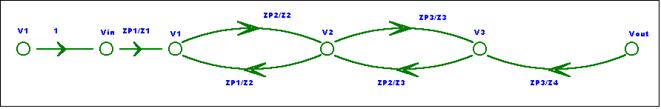
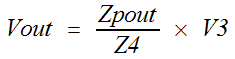
The last node is Vout. Vout is also a summing
node.
ZPout =
Z4 // ZL
The SFG is complete. The sequence of loops is
characteristic of a ladder network. Note that each series
impedance creates a loop. Z1 does not create a loop because the input is
a voltage source and the gain of the branch from V1 to Vin
has a gain of zero and is not shown. You can add more rungs to the ladder
circuit via additional series loops.
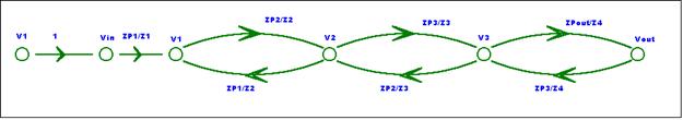
SFG Check
Before analyzing the SFG, check the SFG. Does
it correctly display the signal flow in the circuit?
Examine each node. The incoming branches
specify the variables that affect the node.
Va is an input. An input is a known value. It should not
depend on any other value. In the SFG, an input should not have any incoming
branches.
Vin is a voltage-controlled node. It should only depend
on voltage sources. It should not have incoming branches from summing nodes.
V1, V2, V3, and Vout are summing nodes. Each
summing node should have an incoming branch from every SFG node that it
connects to. The numerator of incoming branch gains should be the parallel
impedance of the node. The denominator should be the connecting impedance.
V1 connects to Vin
via Z1. The SFG should contain a branch directed to V1 with gain ZP1/Z1. V1
also connects to V2 via Z2. V1 should have an incoming branch with gain ZP1/Z2.
Repeat the above for V2, V3, and Vout.
An alternative to the incoming branch check
is the component check. Is each component properly modeled in the SFG?
Each impedance can couple signals in two directions. If the circuit
contains an impedance between node 1 and node 2, the
SFG should contain a branch from V1 to V2 and a branch from V2 to V1. Zero gain
branches and branches to and from the ground node are not shown on the SFG.
The circuit contains an impedance
Z1 that connects Vin and V1. Since the node impedance of Vin
is equal to zero, the branch from V1 to Vin is not shown.
Z2 connects V1 and V2. The SFG should contain
branches from V1 to V2 and from V2 to V1. The gain of these branches is the
destination node impedance divided by the connecting impedance.
In a similar manner, Z3 connects V2 and V3.
Z4 connects V3 and Vout.
There should be a correlation between the
circuit schematic and the SFG.
The above contains lots of checks. Don’t skip
this step. VSA is very simple, too simple. You can easily make a mistake, if
you don’t follow the steps in extreme detail.
Analyze the SFG
The SFG shows a single path from V1 to Vout.
The SFG also shows three Loops. This circuit has lots of interactions. The
interaction is caused by the bidirectional signal flow thru Z2, Z3, and Z4.
Let’s find the loop gains.
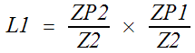
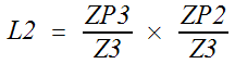
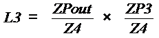
L1 and L3 are non-touching loops. This
creates an interaction between the simple interactions.
The determinant is:
D = 1 – (L1 + L2 +
L3) + (L1 * L3)
The SFG contains one path from Va to Vout. The Path Gain is
The path gain requires a correction for the loops.
No numerator correction is needed since the path touches all the loops. The
transfer function from Va to Vout is:

Substituting for the loop gains and Parallel
Impedances will make the answer far more complex.
Check the Answer
The answer should give the correct result for
all component values. The SFG represents a class of circuits. You can reduce
the circuit to a simple form by removing components and verify that the
equation applies. Try shorts and opens that are easy to analyze.
Does the answer fit your circuit intuition?
In the circuit, Z1 connects the input to node
1. If Z1 becomes an open circuit, than no signal is coupled
from the input to the output. You can open Z1 by making its component
value equal to infinity. If Z1 is infinite, the gain should be equal to zero.
The ZP1/Z1 term creates this result.
In a similar manner, setting Z2, Z3, or Z4
equal to infinity should produce a gain of zero.
The short circuit check can be used for
impedances that connect a node to ground. Z6 connects between node 1 and
ground. If Z6 is equal to zero, it will force V1 equal to zero and force the
input to output gain equal to zero. Z6 is included in ZP1. Setting Z6 equal to
zero will force ZP1 to be equal to zero. A check of the gain formula indicates
that the gain is equal to zero.
In a similar manner, shorting Z5, ZNC5, and
ZL should also produce zero gain.
Some checks can produce indeterminate
results. For example, shorting Z1 will force the value of Z1 and ZP1 equal to
zero. This creates a zero divided by zero term in the gain. Try to avoid these
cases.
The transfer function applies to any
impedance values. It needs to have terms that create the correct value for
shorts and opens. Don’t assume that the equation is correct. Test the answer
and ask how did VSA create the result?
Summary
VSA Analysis only derives the answer in a
simple manner. No claims concerning the answer complexity are made. Use a math
program to evaluate the answer. The Analysis technique allows a simple check of
the answer. Don’t skip this step!
The VSA procedure is summarized below. The
circuit is reduced to a general form, by dropping component values and lumping
components into impedances. The SFG is constructed from the schematic. Mason’s
Gain Formula is used for the output formula.
|
Circuit |
Signal
Flow Graph |
|
|
ZP1=Z1//Z6//Z2 ZP2=Z2//Z5//Z3 ZP3=Z3//Z7//Z4 ZPout=Z4//Zl
|
In this example, the general gain equation for
a ladder circuit was derived. The gain from an input voltage to the output
voltage is given via the Vout/Va equation. The
analysis can be extended to larger ladder circuits. Note the pattern of the
output equation.
The terms in the numerator represent simple
circuit gains. ZP1/Z1 is the circuit gain from the input to node 1, if node 2
is grounded. ZP2/Z2 is the sub-circuit gain from node 1 to node 2, if node 1 is
an ideal voltage source and node 3 is grounded. Etc. This is a simple circuit
with a large correction for interactions.
The SFG was constructed from simple circuit
gains. The gains on the SFG represent circuit gains if no interaction is
present. The circuit is a bit more complicated. Instead of trying to understand
the interactions, VSA lets Mason provide the corrections.
A ladder circuit has been analyzed many
times. With a bit of luck, you may find a general equation. With K9 it can be
easier to derive the circuit equation than perform a search.
Conclusion
Equations
are easy to derive.
Accurately
model the circuit. Inputs and loads must be defined.
Don’t
let the schematic scare you. Model reactive components as
impedances.
Don’t
analyze a specific circuit. Look for a general form to get a broader answer.
Transform
the circuit schematic into a SFG. Brandy’s Gain Formula
supplies the branch gains.
The
SFG gains may require corrections. Let Mason handle any circuit interactions.
Check
the result.
Input and output impedance equations can be
derived as the gain from a current to a voltage. Look at the Ladder Input Impedance Example.